
mask applied in Flexible printed circuit
Solder mask application is a critical step in the manufacturing process of flexible printed circuits (FPCs), serving to protect conductive traces, prevent solder bridging, and enhance the reliability of the circuit assembly. Unlike rigid printed circuit boards (PCBs), where solder mask is typically applied using a subtractive process, the application of solder mask in FPCs often involves a combination of additive and subtractive techniques to accommodate the flexible nature of the substrate.
The first step in applying solder mask to an flexible printed circuit involves surface preparation to ensure proper adhesion and coverage. The flexible substrate, typically made of polyimide or similar materials, is thoroughly cleaned and treated to remove contaminants, residues, and oils that could interfere with the adhesion of the solder mask material. Surface treatment methods may include plasma etching, chemical etching, or mechanical abrasion, depending on the specific characteristics of the substrate material.
Once the substrate is prepared, the solder mask material is applied to the surface using a variety of techniques. In some cases, a liquid photoimageable solder mask (LPSM) is screen-printed or sprayed onto the substrate in a thin layer using precision equipment. The LPSM is then cured using ultraviolet (UV) light or heat to harden the material and create a protective coating over the conductive traces. Alternatively, a dry film solder mask (DFSM) may be laminated onto the substrate using heat and pressure, followed by exposure to UV light to cure the material.
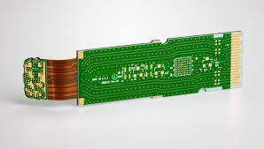
How is solder mask applied in Flexible printed circuit?
After the solder mask material is applied, the next step involves patterning and curing to create openings or windows in the mask layer for exposed solder pads and vias. This process typically utilizes photolithography techniques, where a photoresist layer is applied over the solder mask material and exposed to UV light through a photomask that defines the desired pattern. The exposed areas of the photoresist are then developed and removed, leaving behind a patterned mask layer that protects the designated areas of the substrate during subsequent etching or plating processes.
In the case of additive solder mask application, the solder mask material is selectively deposited onto the substrate through a stencil or mask, followed by curing to harden the material. This method allows for precise control over the deposition of solder mask material, making it suitable for applications where fine pitch traces or complex geometries are present. Additive solder mask application is often used in combination with subtractive techniques to achieve the desired coverage and resolution on the FPC.
Subtractive techniques involve the removal of excess solder mask material from the substrate to expose the underlying copper traces and pads. This may be accomplished using chemical etching, laser ablation, or mechanical milling processes, depending on the specific requirements of the design and the desired level of precision. Once the excess solder mask material is removed, the FPC is thoroughly cleaned and inspected to ensure that the solder mask layer conforms to the design specifications and quality standards.
In conclusion, solder mask application is a critical step in the manufacturing process of flexible printed circuits, serving to protect conductive traces, prevent solder bridging, and enhance the reliability of the circuit assembly. By employing a combination of additive and subtractive techniques, manufacturers can achieve precise control over the deposition and patterning of solder mask material, ensuring optimal performance and functionality in a wide range of applications.