
Via in Pad Affect Board Thickness
Vias are essential to PCB design because they allow signal routing between layers. However, they are not without their challenges. For example, a via’s walls can introduce inductance into the signal, which affects its frequency response and can cause circuit board failure.
One way to reduce inductance is to use a via-in-pad, which provides a smoother transition from a pad to the connecting trace. In addition, it can help eliminate the need to route signals from a pad to another layer and improve signal quality. However, there are a number of important things to consider when using this technique.
A via in pad (Via in Pad Plated Over) or VIPPO is a type of PCB via that is plated over and filled with epoxy. These are typically used in high density Surface Mount Technology (SMT) components like Quad-flat No Leads (QFNs) and Ball Grid Arrays (BGAs). The purpose is to prevent solder wicking down the via’s barrel, which can weaken the joint with the component’s lead and create a potential electrical short.
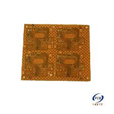
How Does a Via in Pad Affect Board Thickness?
To avoid this problem, the via holes are plugged before the assembly process. This is done with a non-conductive epoxy. Conductive epoxies are also available for applications where the via is carrying a lot of current or heat. Once the epoxy is cured, it is planarized and then plated over to form the V-in-Pad. This type of via adds cost and complexity to the board, but it can prevent wicking, outgassing and other manufacturing defects from occurring during the assembly process.
In addition to reducing inductance, the V-in-Pad can improve signal integrity by eliminating the need to route from a pad to a different layer. This can be useful for high-frequency nets that require a smoother transition. It can also simplify the overall design by allowing designers to reduce the number of traces and reduce copper usage on the board.
When using a V-in-Pad, the design engineer must take into account the pad size and the manufacturing tolerances for the device footprint. The pad size must be large enough to accommodate any drill wander and to leave sufficient copper space around the edge of the hole to meet IPC minimum annular ring requirements.
In conclusion, via in pad is a powerful technique in modern PCB design that addresses the demands of miniaturization, enhanced electrical performance, and thermal management. While it introduces challenges in terms of manufacturing complexity and cost, its benefits often outweigh these drawbacks in high-performance and space-constrained applications. As technology continues to advance, the adoption of via in pad is likely to grow, becoming an indispensable part of cutting-edge electronics design.
In addition, the diameter of the pad should be large enough to allow for a via of the correct size. Using a smaller pad can result in the formation of a bridge on the bottom side of the PCB, which can cause signal problems when the circuit is operating. The pads should also be designed with enough thickness to prevent damage when the component is removed from the V-in-Pad.


